Update January 10th 2012
Update January 10th 2012

|
Burignat, S. & De Vos, A. "Test of a Majority-based Reversible (Quantum) 4 bits Ripple-carry Adder in Adiabatic Calculation", Proceedings of the 18th International Conference "Mixed Design of Integrated Circuits and Systems" (MIXDES~2011), 2011, pp. 368-373 |
BibTeX |
Test of a majority-based reversible (quantum)
4 bits ripple-carry adder in adiabatic calculation
Stéphane Burignat and Alexis De Vos
Universiteit Gent,
Vakgroep elektronika en informatiesystemen
Sint Pietersnieuwstraat 41
B - 9000 Gent
Belgium
Email: research@burignat.eu; alex@elis.ugent.be
Abstract— Quantum computing and circuits are of growing interestand so is reversible logic as it plays an important role in thesynthesis of circuits dedicated to quantum computation. Moreover,reversible logic provides an alternative to classical computingmachines, that may overcome many of the power dissipationproblems in the near future. As a proof of concept we designedand tested a reversible 4 bits ripple-carry adder based on ado-spy-undo structure. This paper presents some performancesobtained with such a chip processed in standard 0.35 μm CMOS technology and used in real reversible calculation (in this study,computations are performed in both directions such that additionand subtraction are made reversibly with the same chip). We alsodiscuss the superiority of using adiabatic signals over classicalrectangular pulses when using dual-line pass-transistor logicgates. Adiabatic signals allow the signal energy stored on thevarious capacitances of the circuit to be redistributed ratherthan being dissipated as heat. Finally, we show that adiabaticsignals allow to avoid calculation errors introduced by the useof conventional rectangular pulses and allow to drasticallyreduce the number of pulse resynchronization in large circuits.
Index Terms—reversible computation, design, implementation,pass-transistor logic, ripple-carry adder, Spectre simulation,quantum computation, adiabatic signal, test and measurement.
I. Introduction
Reversible computing is useful both in lossless classical
computing [1] and in quantum computing [2]. Reversible
circuits also present less power consumption against classical ones
[3, 4, 5].
The physical implementation of the adder we are presenting is
reversible dual-line complementary pass-transistor CMOS logic
[6] and does not make use of buffer of any sort nor level
restorer. This adder has been extended and embedded in larger
components such as a multiplier [7] and, more recently, in a H264/AVC encoder [8].
We present for the very first time to our knowledge, extensive
electrical tests performed on a reversible CMOS chip computing
in both directions: forward (adder) and backward (subtractor) and
compare the efficiency of both classical rectangular pulses and
adiabatic signals.
II. Short history and description of the reversible adder chip
In 2005, Cuccaro et Al.
[9] presented a new linear-depth
ripple-carry quantum addition circuit making use only
of controlled-NOT (CNOT or Feynman) gates and
controlled-controlled-NOT (CCNOT or Toffoli) gates which was
an improved version of a V-shaped reversible adder presented by
[10]. In 2008, [7] presented the synthesis and design of a
reversible Fourier transform making use of such a reversible adder,
but using a do-spy-undo (majority-unmajority) scheme structure as
firstly presented by [11]. This design was making use only of
controlled-NOT (Feynman) gates and controlled-SWAP (Fredkin)
gates1 .
Unfortunately, this 8 bits adder was embedded in a larger
8 bits multiplier making it impossible specific access to
measurements.
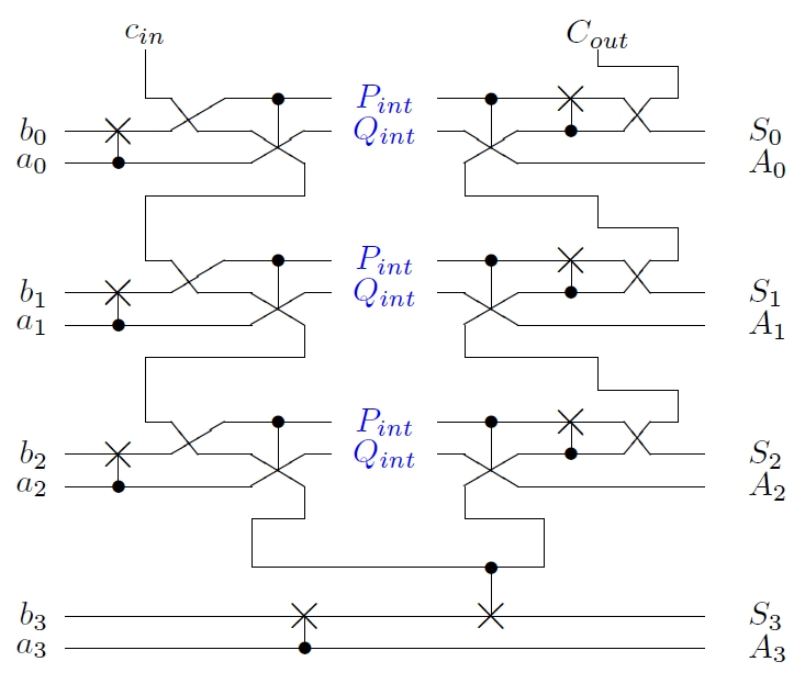
The circuit we present in this paper is a 4
bits majority-based
reversible ripple-carry adder. As in [7], it makes use only of
Feynman and Fredkin gates and presents, as a general structure, a
do-spy-undo scheme [11]. Full details about synthesis
discussion, structure and theoretical consumption are already
presented in [12].
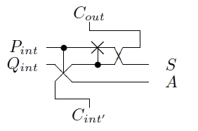
As a summary, let us recall the block structure of the studied
adder. Let n denote the size of both numbers to be added. First,
as a do-spy-undo structure is used, each bit addition implemented,
except the most significant bit (MSB), necessites one do-undo
circuit. The 3 inputs majority do circuit and the 3 inputs
unmajority undo circuit are presented in Fig.1 and Fig.2,
respectively.
The do-undo block constitutes a one bit adder when used
forward (respectively a one bit subtractor if used backward). The
numbers a and b (respectively S and A) are the main inputs and
Cin (Cout) is the carry-in. The number S (b) represents
the computation result (sum a
+
b respectively difference
S
-
A) and A (a) is a copy (garbage) of the input a (A) and
so is the output Cout (Cin) with respect to the input Cin
(Cout).
When an addition is computed (forward calculation), the
internal bits Cint are used for carry transmission from one stage
to the next during the majority operations, while the input Cint
′
of the undo block rebuild the initial input cin during the undo
operations (Cout =
cin). When a difference is computed
(backward calculation), the inverse process occurs leading to the
calculation of the difference.
For 1 bit calculation, Cint would be directly connected to
Cint
′ whereas if the adder size n
≥
2, the most significant bits
addition is performed by using only two Feynman gates; one is
used to compute the bit sum XOR (⊕) and the other to
sum-up the carry to the final result. Each extra bit addition is
realized by cascading supplementary do-undo blocks, linked
together by connecting Cint to cin and Cout to Cint
′ as
presented in the full schematic of the 4 bits adder in Fig.3.
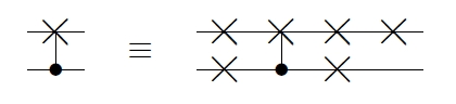
Let us notice that simplification presented in Fig.4 has been
used for the real design of the unmajority block.
This 4 bits Cuccaro adder has been designed using the
Cadence© computer-aided design environment software. Each
electrical simulation has been performed using its Cadence
Spectre© simulator (see Fig.7 and Fig.8 as examples).
The chip processing has been realized at ONSemiconductor
through the Europractice
/ IMEC consortium in 350 nm
standard CMOS technology. The transistor lengths used are
L
= 350
nm, both for n-type and p-type transistors, while
widths are respectively Wn = 500
nm and Wp = 1500
nm.
The chip contains a total of 160 transistors (80 n-type and
80 p-type).
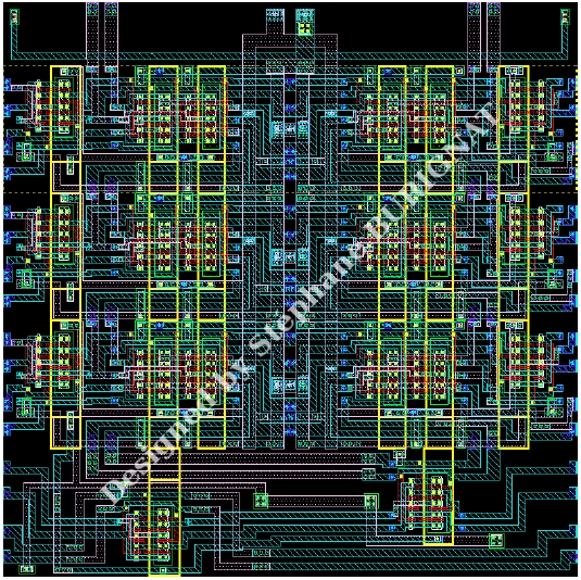
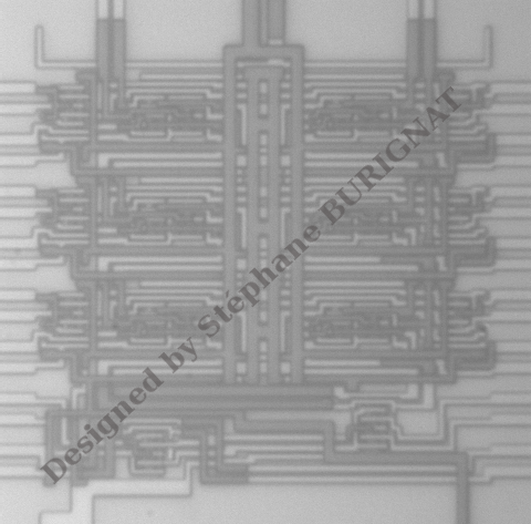
The Cadence Layout of the studied adder is shown in
Fig.5 while Fig.6 presents a photograph of the realized chip
(90
μm
x
90
μm). We can easily recognize the dual inputs and
outputs at each left and right hand sides, and the two dual carries
Cin and Cout at the top side while in the middle part are the
wider wires used for the substrate and the N-wells biasing
(typicaly, V SS =
-
1
.
2
V and V DD = 1
.
2
V ).
Starting with the simulation, two different types of signal have
been used: ”traditional” square pulses and quasi-adiabatic
triangle pulses.
The maximal signal voltages used, both for simulation and for
measurements are V + = 1
V for logic ”1” and V - =
-
1
V for
logic ”0”.
If the first type of signal (square pulse) is applied, for the
unchanged bits, the voltages corresponding to the desired logic
levels remain constant while others are fastly switched. If the
second signal type (adiabatic) is applied, a triangular pulse ranges
from Let us stress that the pulses of Fig.7 are representative of the
input signals previously defined. Fig.8 presents the corresponding
difference
b and garbage
a calculated outputs when using the
Cuccaro adder in reverse mode (subtractor), for both the square
and triangle adiabiatic pulse shapes. In Fig.8, we see that
rectangular pulses do not all have the same amplitude, that they
are also presenting large transition peaks while for the triangle
adiabatic signals, the pulses are regular, without any transition
peak.
Let us also notice that when the size n of the numbers to be
computed is larger than two, some exceptional errors may occur
when square signals are used while this doesn’t happen when
adiabatic signals are applied (Fig.8
).
One reason for that comes directly from the transmission gate
that is build of two complementary transistors in parallel. Due to
the steep slope generated during the transition of the square pulse,
if a delay occurs between the control signals on the transistor
gates and the signals transmitted through the transistor channels,the gates do not shut down the signal at the very moment of the
transition and an opposite signal that would have been cut
down is transmitted anyway, occasionally causing calculation
errors.
If the adiabatic signals are used, the smooth transitions allow a
delay between the signals. In effect, during the transition
steps, the two transistors are working below their threshold
voltages, drastically lowering the amplitude of the output signal
(see also Fig.10 and comments). As the example of Fig.9
shows, a phase difference – expressed as a percentage of the
period – as large as a quarter of a period PrcT
=
±
25
%
(plain lines) does not introduce any calculation errors, even
if the final shape of the signal is deformed and if some
small variations of the output potential (inferior to 40
mV )
appear when the transmission gate is closed. In fact, this
maximal percentage will be dependant of the ratio between the
maximum pulse voltage and the pseudo-threshold voltage of
the transmisson-gates used. When a bigger phase appears,
the output signal is no more zeroed before the command
pulse.
A positive (respectively negative) phase indicates a
delay of the input (respectively command) signal with
respect to the command (respectively input) pulse
2.
Further in the calculation steps, the signals may become
symmetrical again, when two phased signals are used successively
as the command and the transmitted signals. This then leads to a
narrowing of the final pulse width (as seen in Fig.8) but does not
impact significantly its maximal amplitude that is related to the
impedance of the circuits. In Fig.9 (dash lines), the simulated
output signal obtained from a single transmission gate when the
phase equals zero (PrcT
= 0
%) is larger than the output signals
obtained from a complex circuit such as a subtractor (Fig.8),
where a phase is introduced by the propagation of the internal
carries Cint and Cint
′. In effect, in the Cuccaro adder, the cin
signal when going through the whole computation, has to be
transmitted twice at each stage of the calculation. The greater
the bit size n, the greater the number of stages, the greater
the phase introduced, the narrower the pulse. When using
a square signal, this may produce wrong pulses whereas
when using an adiabatic shape, the signal will be deformed,
narrowed, but the calculation will remain possible with very
few loss in amplitude and still guaranteeing a correct logic
“1” or correct logic “0”. This was checked up to n
= 6
bits.
It is also easy to verify that dual signals (e.g. a and ) are
closely synchronized by symmetry of the dual circuits – each
signal and its complementary having passed through the same
number of transmission gates.
As a consequence, even if we need to pay attention to the
design of the circuit in order to limit the phase introduced
between the different signals used in the calculation, the triangular
adiabatic shape signals allow to drastically reduce the number of
level restorers and pulse resynchronizers.
Several extensive measurement steps have been performed on
the Cuccaro circuit, both in forward (adder) and in reverse
(subtractor) calculations.
Constant voltage computations are primary presented allowing
to bring information principally on impedance and voltage bias
impact on calculation. In a second hand, we present the adiabatic
generator used for the experimental application of the input
pulses. We then present measurements of the outputs obtained
both in direct and reverse calculations.
A. Preliminary DC measurements
The voltages applied: substrate and NWELL biases, input
constant biases, have been measured using a Flucke
175
multimeter in DC mode.
A large part of the truth table has been first successfully
checked and some measurements have been done for some
particular conditions:
From these measurements, the maximum voltage drop found for
the adder is 30
mV whereas the maximum voltage drop for
subtractor was found to be 6
mV over a constant input bias of
1
V . In any cases, the output drops are inferior to 3
% of the
input signal biases which is the order of magnitude of the
measurement incertainties.
Fig.10 presents a typical variation of an input voltage as a
function of the output voltage bias when the adder is used in
reverse mode (i.e. as subtractor). In fact, same curves are obtained
for each output whether in direct mode (adder) or reverse one
(subtractor), except for the most significant bit A3 (respectively
a3) that is made by a direct connection to its corresponding input
a3 (respectively A3) (see Fig.3). For all measurement performed,
the voltages V DD and V SS =
V GND are kept constant to 1
.
2
V
and -
1
.
2
V respectively.
We see from Fig.10, that a minimal voltage input as small as
420
mV can still be used (without security marge) to perform
calculations with this Cuccaro chip. This is also coherent with the
general shape of simulated output pulses in Fig.8 and with the
experimental measurements in Fig.12 and Fig.13 that present the
same transition when applying a linear input variation (triangular
adiabatic pulse). But in these last cases, one also needs to
account for the impact of the phases introduced by the internal
carry signals that not only narrow the pulse width but also
slightly increase the minimal voltage input possibly used to
perform a calculation. We then arbitrarily fix the limit of
±
500
mV as the minimum logical amplitude acceptable to
define a logic ”1” (above 500
mV ) or a logic ”0” (below
-
500
mV ). This choice is experimentally driven by the
fact that within these two defined domains, the calculated
signals obtained have always been found conform to what was
expected.
The pseudo-threshold
voltage3
V pT of the Cuccaro adder is found to be about 350
mV which is
also close to the simulated value of the transmission-gate
pseudo-threshold voltage. Between about 420
mV down to
V pT = 350
mV a transition occurs that corresponds to the linear
mode of the transmission gate transistors. Below V pT, the
transmission gates are blocked and, as expected, no signal is
transmitted.
B. Generation of the adiabatic signal
In order to apply the necessary adiabatic pulses, we designed
an electronic module allowing to genetrate 4 types of triangle
pulses:
These four signals are all build up from one single triangular
pulse ranging between +1
V and -
1
V by using a single
buffer (switching pulse), an inverter followed by a buffer
(dual switching pulse) or using a precision full-wave rectifier
followed either by a buffer or by an inverter and a buffer (logic
”1” and logic ”0” respectively). Fig.11 presents the full
schematic of the electronic module used to generate the
experimental adiabatic pulses. It is a very simple thus very
accurate circuit presenting very low output impedances. The
operational amplifiers are polarized at ±
3
V while the input
triangular signal has an amplitude of 2
V . This allows the
operational amplifiers to work in the linear part of their
characteristics and gives very accurate and reproducible
pulses.
AC measurements have been performed using a commercial
TektronicsTM TDS
210 digital oscilloscope. The output charge is its
×
1 probe that can be modeled by a 1
M
Ω resistor in paralell
with a 32
pF capacitance.
By using the voltage divider technique, the experimental output
impedance of the Cuccaro adder (or subtractor) is found to be
Zout ≃
5250
Ω
±
5
% whereas it is found to be close to 8
k
Ω
by Cadence Sperctre© simulation.
Fig.12 and Fig.13 show typical experimental measurements
realized respectively in forward (adder) and backward (subtractor)
computation.
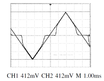
Experimental Measurements in forward computation –
In Fig.12, the dual output (
S3,
S3
) is given as the example of a
constant logic “1“ adiabatic output and compared to the
switching input a0. For clarity, the dual signal S3 that is
a logic “0“ is also compared to the same input a0 – the
complementary a0 being the exact opposite signal of a0
(a0 =
-
a0).
As previously found in Fig.10, the impact of the threshold
voltage can be seen on both dual output signals in Fig.12, at
the rise front whereas at the descending one, its impact is
superimposed to capacitance effect coming from the probe that
slows down the decrease of the signal to the mean value Experimental Measurements in backward computation
–
As shown in Fig.13, very similar results are obtained when
performing a subtraction using the same chip in reverse direction.
Here, the output calculated (
b3,
b3
) signal, shown as typical
example, is a constant dual zero also compared to the same input
signal A0.
As the carry propagates twice through the whole circuit, a
maximal delay is obtained between the two extreme output bit
pulses (e.g. a0 and b3). The maximum delay τ
= 91
μs is
measured between outputs a0 and b3 during a subtraction
(Fig.14
). This delay is obtained between two pulses at a frequency
120
Hz, when probes are connected to the outputs. According to
these measurements, it is possible to cascade more than 23
Cuccaro gates before the output delay reaches 25 % of the period
such that calculation errors may appear.
Cascade Measurement –
Example of switching signal measured on cascaded circuits As a last experiment, we cascaded an adder with a subtractor.
This experiment allowed to verify that two sequential calculations
can be performed and that the addition can really be uncomputed
giving back the initial input signal as in the example given in
Fig.15.
A large part of the identity truth table (different from the first
experiment) has been checked with no errors detected. Also, no
significant extra phase nor attenuation occured during this
computation steps, giving the indication that a lot of reversible
chips may be cascaded.
Nevertheless, the output signal having been transmitted through
several transmission gates is not the exact input signal, but a
calculated one and inherit of the same characteristics than another
calculated output.
We presented real calculations performed in a 350
nm CMOS
technology reversible (quantum) adder used in both direction:
forward adder and backward subtractor.
The superiority of making use of adiabatic triangle pulses has
been demonstrated and explained, showing that using adiabatic
pulses on pass-transistor based reversible (quantum) chips is a
suitable solution to perform linear calculations.
Acknowledgment
The authors thank the Danish Council for Strategic Research
for the support of this work in the frame- work of the MicroPower
research project. They are grateful to the Invomec division of Imec
v.z.w. (Leuven, Belgium) and the Europractice consortium for the
help with the prototyping of the chips.
References
 to the desired logic level at each calculation step.
Thus, in case of the second signal type, all signals (i.e. both the
unchanged bits and the changing ones) temporarily come to
the equilibrium voltage, half-way logic ”1” and logic ”0”.
The two signal types can be seen in Fig.7 presenting the
minuend
S and subtrahends
A of nine subsequent subtractions
S
-
A.
to the desired logic level at each calculation step.
Thus, in case of the second signal type, all signals (i.e. both the
unchanged bits and the changing ones) temporarily come to
the equilibrium voltage, half-way logic ”1” and logic ”0”.
The two signal types can be seen in Fig.7 presenting the
minuend
S and subtrahends
A of nine subsequent subtractions
S
-
A.
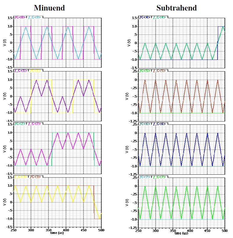
Fig. 7. Cadence Spectre© simulation: comparison of rectangular and adiabatic input pulses of same frequency.
Top line is the least significant bits
S0 and
A0 whereas the bottom one corresponds to the most significant bits
S3 and
A3.
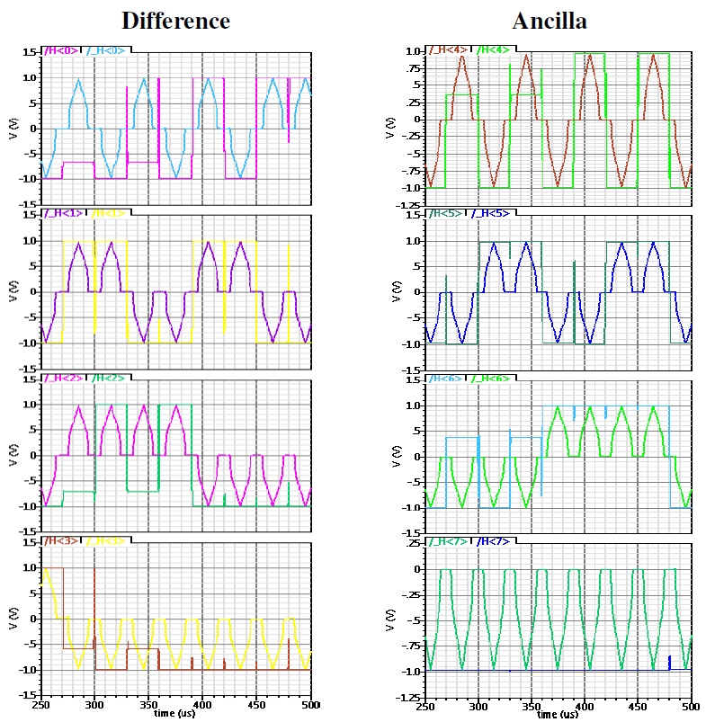
Fig. 8. Cadence Spectre© simulation: comparison of the output signals
when using rectangular and adiabatic pulses, respectively.
According to Spectre© electrical simulation software, using rectangular pulses introduces
several errors in computation.
None of these errors occur when using triangular pulses.
Top line is the least significant
b0 and
a0 bit whereas the bottom one
corresponds to the most significant ones
b3 and
a3.
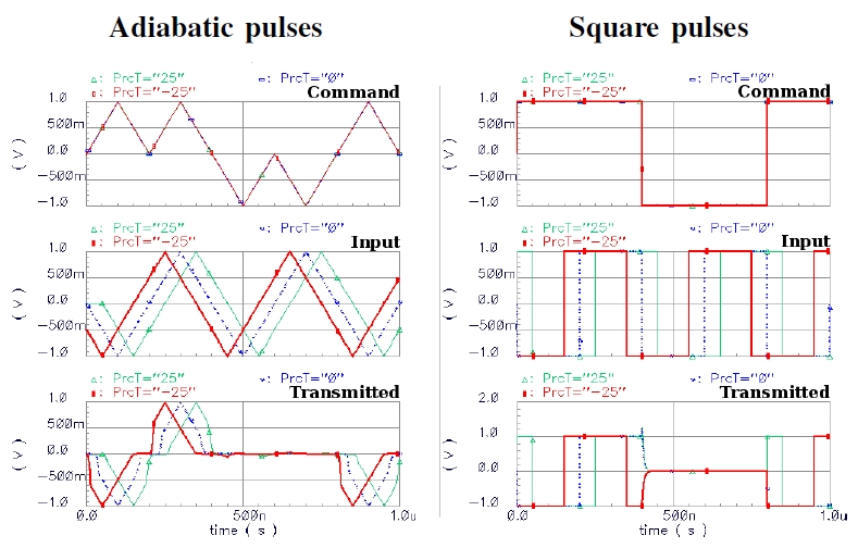
Fig. 9. Cadence Spectre© simulation of a complementary pass transistor
gate: comparison between adiabatic and square pulses when a dephasing
of
PrcT
=
-
25%
(bold) and
25%
of the period is applied between the
command pulses and the signal to be transmitted.
The dashed lines correspond
to a phase equal to
0
%
. The frequency used is 5 MHz.
Fig. 10. Measurements of the input voltage dependance of bit
b2 as a
function of the output voltage bias of bit
S2, for the reverse (subtractor)
calculation:
b
=
S
-
A
= 0110
-
0
1
01 = 0
0
01
.
 up to +1
V and back,
up to +1
V and back,
 down to -
1
V and
back,
down to -
1
V and
back,
 .
.
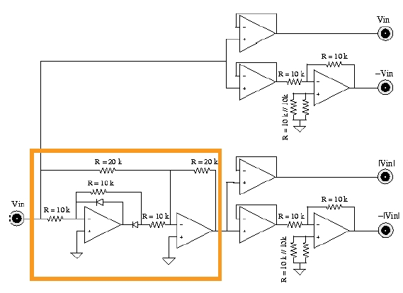
Fig. 11. Electronic schematic of the adiabatic signal generator module
embedding an accurate full-wave rectifier (framed).
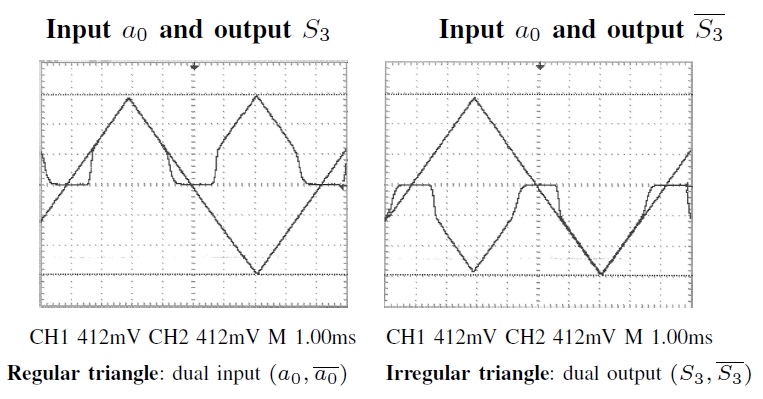
Fig. 12. Oscilloscope snap-view of the
4th dual bits
(
S3,
S3
) as a function
of the dual switching input bits
(
a0,
a0
) = (
X,
X
)
,
obtained by direct (adder)
calculation of
S
=
cin +
a
+
b
= 1 + 011
X
+ 0110 =
1
1
X
X (with
cin = 1
), measured when using adiabatic pulses.
 here equal to zero, while all the transmission gates of the chip are
reaching their open circuit functionality.
here equal to zero, while all the transmission gates of the chip are
reaching their open circuit functionality.
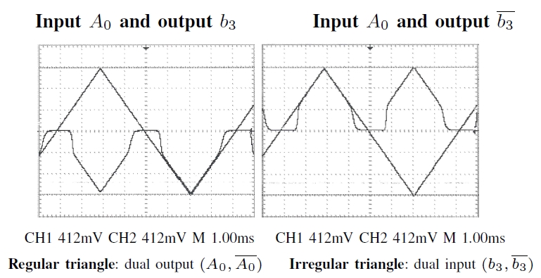
Fig. 13. Oscilloscope snap-view of the
4th dual bits
(
b3,
b3
) as a function
of the the dual switching bits
(
A0,
A0
) = (
X,
X
)
,
obtained by reverse
(subtractor) calculation of
S
-
A
=
b
= 0110
-
010
X
=
0
0
X
X
with
Cout = 0
and measured when using adiabatic pulses.
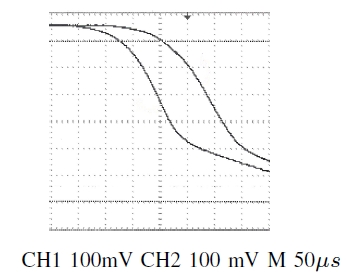
Fig. 14. Experimental
maximum phase introduced during
a computation step. Top line
:
b3,
Bottom line
:
a0.
Fig. 15. Typical adiabatic
switch of input and output signal
obtained on a cascaded circuit
formed by an adder followed by a
subtractor
 class="newline" />
Regular triangle: dual input
(
a0,
a0
)
,
Irregular triangle: dual output
(
A0,
A0
)
(do-undo computation).
[1] De Vos A.,
Lossless computing
, Proceedings of the IEEE Workshop on
Signal Processing, Pozna
ń (2003) pp.7–14.
[2] Feynman R.P.,
Quantum mechanical computer
, Optics News 11 (1985)
pp.11–20.
[3] Landauer R.,
Irreversibility and heat generation in the computing process
,
IBM Journal of Research and Development 5(3), (1961) pp.183–191.
[4]
Bennett C.H.,
Logical reversibility of computation
, IBM Journal of
Research and Development 17(6), (1973) pp.525–532.
[5]
Toffoli T.,
Reversible computing
, in: Automata, Languages and
Programming, ed. by W. de Bakker, J. van Leeuwen (Springer,
Berlin, 1980), Technical Memo MIT/LCS/TM-151, MIT Laboratory for
Computer Science (1980) pp.632-644.
[6]
De Vos A.,
Reversible computer hardware
, Electronic Notes in
Theoretical Computer Science 253, (2010) pp.17–22.
[7]
Skoneczny M., Van Rentergem Y. and De Vos A.,
Reversible Fourier
transform chip
, Proceedings of the 15th International Conference on
Mixed Design of Integrated Circuits and Systems (MIXDES 2008),
Poznań, June 2008, (2008) pp.281–286.
[8]
De Vos A., Burignat S. and Thomsen M.K.,
Reversible implementation
of a discrete integer linear transformation
, Proceedings of the 2nd
Reversible Computation Workshop, Bremen (2010) pp.107–110.
[9]
Cuccaro S., Draper T., Moulton D. and Kutin
S.,
A new quantum ripple-carry addition circuit
, Proceedings of the 8th
Workshop on Quantum Information Processing, Cambridge (June 2005),
arXiv:quant-ph/0410184v1 (2004) 9 pages.
[10]
Verdal V., Barenco A. and Ekert A.,
Quantum networks for elementary
arithmetic operations
, Physical Review A 54 (1996) pp.147–153.
[11]
Fredkin E. and Toffoli T.,
Conservative logic
, International Journal of
Theoretical Physics, 21 (2004) pp.219–253.
[12]
De Vos A.,
Reversible Computing
, WILEY-VCH (2010) 251 pages.
[13]
Van Rentergem Y. and De Vos A.,
Optimal design of a reversible full
adder
, International Journal of Unconventional Computing 1 (2004)
pp.339-355.